About the internal structure of SDRAM
We borrowed some of the text from the Advanced Advanced Memory Technology Guide to explain:
SDRAM is actually a storage array. You can imagine that if SDRAM is not in the form of an array but in the form of a pipe, SDRAM is difficult to achieve random access. . The array is like a table, filling in the data. As with the retrieval principle of the table, first determine a row (Row), and then determine a column (Col), we can accurately find the required cell, which is the basic principle of memory chip addressing. For memory, this cell can be a storage unit, so what is this table (storage array) called? This is the logical bank (Logic Bank, hereinafter referred to as Bank).
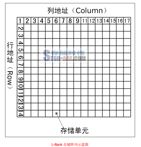
Seeing this, everyone should not imagine that the way we address SDRAM is: first determine the address of the bank, then determine the address of the row and column.
SDRAM memory capacity calculation method
Regarding the calculation of memory, let's look at the manual first.

The 128Mb in the figure indicates the total capacity of the SDRAM. 2M: indicates that 1 bank has 2M addresses, that is, one bank has 2M memory cells; 4Bank indicates 4 banks; 16 I/O means that the bit width is 16 bits, the data bus uses 16 bits, and the maximum number that a memory cell can store is 2^16-1=65535. Then calculate the capacity according to each parameter: 2M x 4 x 16b = 128Mb.
SDRAM chip pin introduction
The first picture is the pin diagram of SDRAM, and the second picture is the description information of each pin signal.

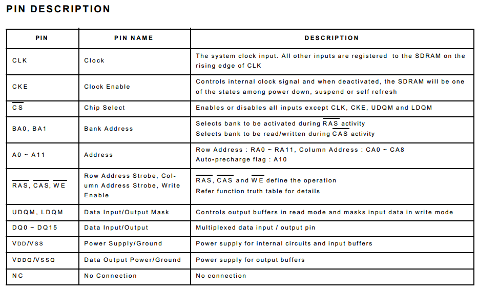
The above two pictures can be found in the manual of the SDRAM chip. Below Kevin, we will briefly introduce the signals that we need to focus on when doing FPGA development.
CLK: The clock for SDRAM operation, and all input signals are detected on the rising edge of CLK, that is, any command we give to SDRAM must be raised in CLK. The edge stays stable so that SDRAM does not get the error when we get the command we gave.
CKE: The clock enable signal is a signal used to control whether the internal clock of the SDRAM is working (there is also a clock inside the SDRAM)
CS: Chip select signal, it should be noted here that if you want to operate on SDRAM, you must lower the chip select signal.
BA0, BA1: Bank address line, used to give the bank address, can control 4 banks of SDRAM
A0~A11: Address line. When we select the Row address of a bank of SDRAM, we need to go to 12 address lines (A0~A11); when we choose the address of Col, only Use 9 lines A0 ~ A8; A10 this signal can be used to control Auto-precharge.
RAS, CAS, WE: These three lines are used to send commands to SDRAM, including initialization, read, write, auto charge and other commands.
UDQM, LDQM: Data input/output mask.
DQ0~DQ15: The data lines of SDRAM are bidirectional. The data written to or read from SDRAM is transmitted on DQ.
You can see that the above address bus A0~A11 can control both row and col, and the number of lines used to control col address and control row address is different. There may be some doubts, Kevin explained to you below:
SDRAM vendors generally use the same bus to address SDRAM in order to save costs.Nothing wrongFor the Row address, 12 lines are used, that is, there are 2^12=4096 Row addresses in total, and the col address uses 9 lines, that is, there are 2^9=512 col addresses, and if added together, A bank has 4096 × 512 = 2,097,152 (2x1024x1024), that is, there are 2M addresses, in this case, it is in line with our previous calculation of SDRAM capacity.
If you have another one, you may not understand the role of the mask (UDQM, LDQM). Please listen to Kevin's explanation below:
Take the SDRAM chip we use, there are 16 data lines, which means that the number of bits of our data can reach 16 bits, but please note that maybe we are When using SDRAM, maybe when we write data to SDRAM, we generate only 8 bits of data, but the FPGA is connected with 16 data lines of SDRAM. At this time, the data stored in SDRAM is still 16 bits. So, in order to avoid this problem, we can use the mask to mask the upper 8 bits. Of course, the role played by the mask when reading data is similar.
SDRAM related operation timing
In front of so much SDRAM related knowledge, I believe that you can't wait to know how to operate SDRAM, you look at the official and listen to Kevin in detail.
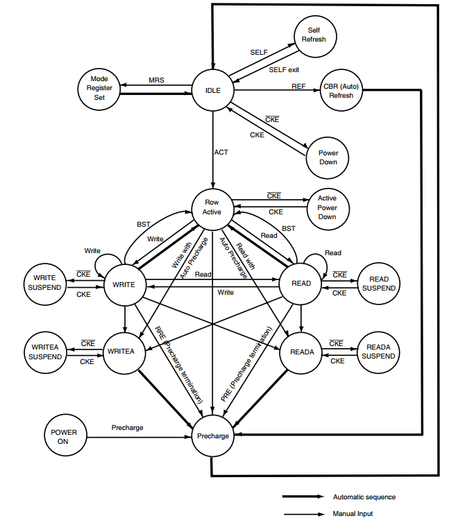
The above picture is a state jump diagram inside SDRAM (the pictures that may be seen on the web page are not very clear, you can download these in the “Documentation Manual” under the navigation menu “Welfare” Document), the thick black line indicates that it will automatically jump to another state in this state, and the thin black line indicates that the command needs to be jumped.
SDRAM initialization
We first find the state of the SDRAM "POWER ON", which is just power-on. After the "POWER ON" status is given to the 'Precharge' command, it will jump to the "Precharge" state and then automatically jump to the "IDLE" state. In the "IDLE" state, we need to give the SDRAM twice the Auto-refresh command, and then we need to set the mode register. After the mode register is designed, our initialization process is over. Having said that, we still don't know how to initialize the SDRAM. At that time, Kevin still didn't know how to write the code to initialize the SDRAM after reading the "Advanced Advanced Memory Technology Guide". In this blog post, Kevin will not talk about how to write code for the time being. I will only explain the timing and principle related to the initialization process. The principle is well understood. I believe everyone will have some idea how to write the code. For a code on how to write, you can also refer to Kevin's other blog post.
We continue to the picture in the official document. This time we can have a waveform diagram. You should look at it carefully. It is very helpful for you to write the code:
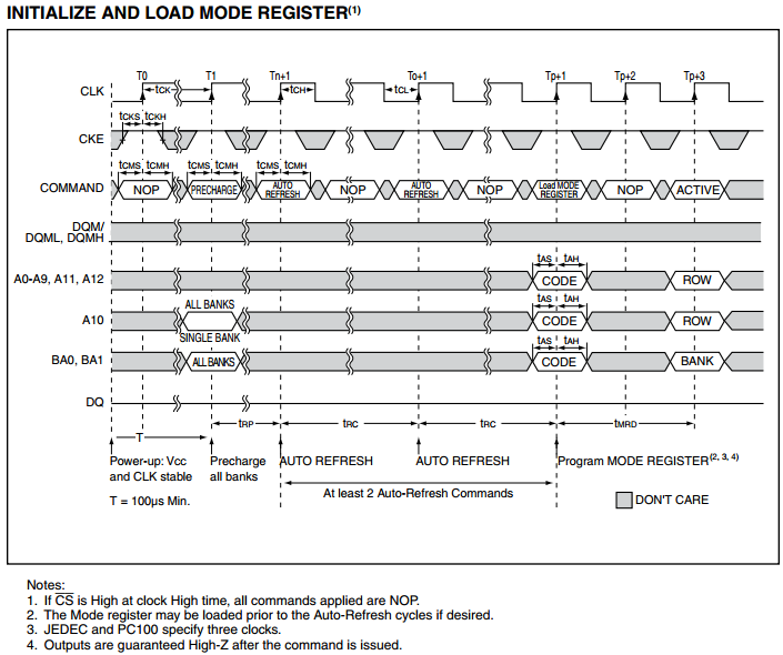
It may be a headache for everyone to come into contact with this timing diagram for the first time, but it doesn't matter. Please listen to Kevin for a slow explanation. While reading the documentation, the status is above. The diagrams are easier to understand. For each instruction that appears in the diagram, we can find it in the device manual we use:
According to the official documentation, SDRAM can not send other commands to SDRAM except for “COMMAND INHIBIT” or “NOP” during the 100us power-on period, so everyone can see the transmission. The minimum interval of the "Precharge" command and the power-on interval "T" is 100us. This 100us is actually equivalent to a stable period of SDRAM. A friend who has read the article "Master Advanced Memory Technology Guide" may find that the stabilizer written in the "Advanced Advanced Memory Technology Guide" is 200us, but here is 100us, so it does not appear. Contradictions, Kevin just appeared in the manual, this question also appeared. What we can be sure of is that the possibility of an official manual error is very small. If even the official documentation is wrong, how can we let those who use their devices live? ( T □ T )╮. Is that the author of the Advanced Advanced Memory Technology Guide wrong? Such a long-tested classic article, if there is a mistake, must have been raised long ago. In the end, Kevin found the answer in the official handbook:
For this English, Kevin understands that SDRAM is likely to execute the "COMMAND INHIBIT" or "NOP" command during 200us, so here we simply get the stabilizer Into 200us. (If you understand the mistake, please criticize it)
After the stabilizer has passed, we will give the "Precharge" command, then the "tRP" time and then the "Auto Refresh" command, and then the "tRC" time. The "Auto Refresh" command is then used for the "tRP" time to set the mode register. When giving the command, we need to pay attention to the fact that the three commands "Precharge", "Auto Refresh", and "Load Mode REGISITER" appear only once, and the "NOP" command is given when these commands are not given. .
When giving the "Precharge" command, we need to specify the A10 and Bank addresses. If A10 is High (All Banks), it means that all banks are pre-charged. To the bank address, if A10 is low (SINGLE BANK), you need to specify the address of a certain bank.
When you give the "Auto Refresh" command, you do not need to specify the bank address (we notice that there is a description in the lower right corner, we do not need to care about the gray part of the data).
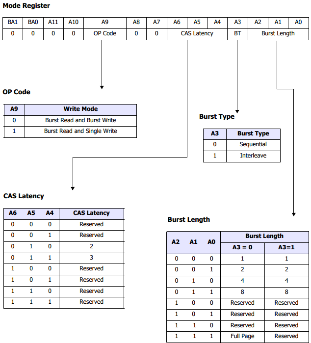
When setting the mode register, the instructions to be given are slightly more complicated. The manual shows A0~A11 and BA0, BA1 is used. Let's see how the mode register should be used. Settings, please see the picture:
A9: Used to specify the operation mode: high for burst read/burst write, low for burst read/single write;
A4~A6: Specify the length of the incubation period. For the incubation period, there is a very detailed introduction to the Advanced Advanced Memory Technical Guide. However, the actual effect of the latency setting is if the latency is set. Yes, when we perform SDRAM read operation, the read data will be delayed by 3 cycles relative to the "READ" command. If the latency is 2, it will be delayed by 2 cycles.
A3: Set the type of burst, continuous and non-continuous.
A2~A0: Used to specify the length of the burst.
For the above explanation, you may think that Kevin may not be straightforward because you don’t understand what is suddenly. Kevin gives an example: A9 is set to 0. The latency is set to 3, the burst type A3 is 0, and the burst length (A2~A0) is set to 4. When we write, the data is written once every 4 data, that is, we give a write command. Will write 4 data into SDRAM, and the four addresses are continuous (if the burst type is set to be non-contiguous, the address will not be continuous, the specific address will be a kind of law, Kevin did not engage himself Understand); when we perform a read operation, after three cycles of giving a read command (latency of 3), four data will collapse continuously.
At this point, for the initialization process, it is basically finished here.
![0@[]7E~02L}W$56V1NH89XT](http://dengkanwen.com/wp-content/uploads/2016/01/0@7E02LW56V1NH89XT.png)
SDRAM write operation
In the state transition diagram, we can see that we need to have a command "ACT" before the initialization or completion of the SDRAM read or write operation (this command is in our initialization sequence). The figure also appears, but we got it here.) The meaning of this command is that the vernacular is the "effective line" command, which is to let a certain line in SDRAM move, so that we can read or write.
Before the official speaking operation, there is still a little hope that everyone can pay attention to it. Maybe a careful friend has already discovered it. In our state transition diagram, there are "WRITE" and "WRITEA". Two states, in these two states, we can write to the SDRAM, just in the "WRITEA" state, after each burst of data is written, the SDRAM will automatically jump out of this state to refresh, and In the "WRITE" state, it is necessary to give the corresponding instruction before jumping out of the "WRITE" state, so in order to improve the running speed of the SDRAM, we generally do not let the SDRAM enter the "WRITEA" state to increase the speed. Of course, the difference between the two states "READ" and "READA" is also the case.
Let's continue with the timing diagram of the previous write operation. This timing diagram does not enter the "WRITEA" state:
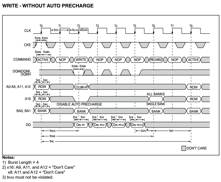
Following the old routine, Kevin continues to work with everyone to analyze the timing of write operations:
After the initialization between the "tMRD", give an "ACT" command, specify which bank of which bank, and then "tRCD" time to "WRITE" "Instruction, at the same time specify the bank address and column address and pull A10 low, and then write the corresponding amount of data according to the set burst length, thus completing our write operation. After writing four data, what is it, this is completely our own decision. If I don't send any instructions to SDRAM, then SDRAM is still in the "WRITE" state. If I want SDRAM to write, then I can send a write command to the SDRAM. If the time to refresh the SDRAM is reached, then we must perform the SDRAM refresh operation to ensure that the SDRAM data is not lost.
It may be seen here that if I am letting SDRAM write data, is it time for SDRAM to refresh, I have to let SDRAM perform refresh operation immediately? This is certainly not a reality. Let's imagine that SDRAM write data is performed every four or four data. If the second data is being written and the SDRAM is refreshed immediately, it will inevitably lose the remaining two data that have not yet been written. On My God, we are categorically unable to let our data be lost. We can't let our data be lost, and we must ensure that the SDRAM is refreshed to ensure that the data in our corresponding SDRAM is not lost. How should we write the code? God, think of it, is there already a friend who has to blow up? Don't panic, how to write code, Kevin will explain in the next blog post, we will be able to thoroughly understand the timing of SDRAM. The timing of the refresh is described later in this article.
The write operation is basically finished here.
SDRAM read operation
Let's talk about our read operation. In fact, the read operation and the write operation are similar. I believe that everyone has the basis of the write operation, and it is easier to understand the read operation of SDRAM. Let's continue with the picture above:
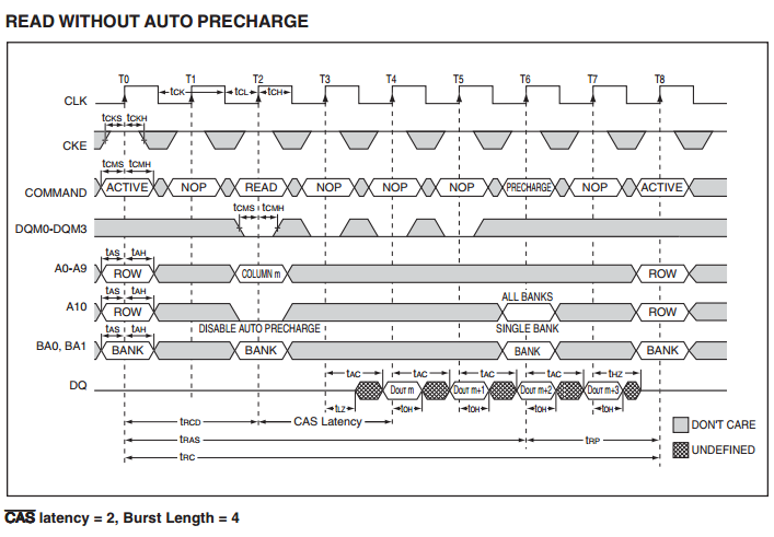
First of all, still give the "ACT" command, remember not to forget to specify the ROW address and BANK address, and then give the "READ" command, after the set latency, our The data is coming out. Don't forget, don't forget the signals on other signal lines when giving the relevant commands.
SDRAM auto-refresh operation
Kevin has mentioned the automatic refresh of SDRAM many times in the past. Why should SDRAM be automatically refreshed? I believe everyone knows the reason through the previous introduction. It can be said that if SDRAM is not refreshed at the time. Refreshing, no matter how much data we write into SDRAM is a no-brainer, so we must pay great attention to the SDRAM refresh operation, and when it is refreshed, it must give a refresh command. The maximum time for SDRAM internal capacitors to save data is 64ms, and we have a BANK with 4096 lines, 64ms/4096~=15us, which means that in order to ensure that the data inside the SDRAM is not lost, the maximum time interval between refreshes is 15us, so in order to allow SDRAM to have more time to read or write, we set the SDRAM refresh period to 15us.
Here, Kevin also wants to add a little knowledge. Every time SDRAM is refreshed, it operates on each row. It does not charge each capacitor separately, so every time it is refreshed, The capacitors in this row are charged and we can understand that they happen synchronously.
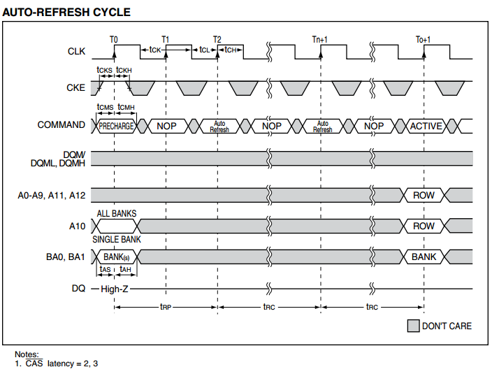
This is the timing chart for SDRAM to automatically refresh. I believe everyone has the previous foundation, and you should not be afraid of this picture.
In each automatic refresh, we need to give a "Precharge" command. What does this command do? You can look at the previous state diagram. If the SDRAM is in the "WRITE" or "READ" state at this time, the "Precharge" command can cause the SDRAM to jump out of the "WRITE" or "READ" state and enter the "IDLE". status. Next, after the "tRP" time, give an "Auto-Refresh" command. Note that we only need to give the "Auto-Refresh" command once.(inElectronic enthusiast forumwithPunctual atom forumIn the post, Kevin wrote the "Auto-Refresh" command twice, which is wrong. I hope to see the friends of this post pay attention to it.At this point, the auto-refresh operation is complete. The automatic refresh operation here is similar to our initialization process, except that there is no setting of the mode register here.
Ok, for SDRAM initialization, reading, writing, and auto-refresh, Kevin has finished all of this based on his own understanding. If there are some errors in this article, I hope you will criticize it in time. In addition, Kevin will share in the next blog post how to write SDRAM controllers, that is, how to write the operations in this article with code.

No comments:
Post a Comment